Pdf Schematic To Pcb
[get 18+] vivo y71 schematic diagram download Pcb schematic common mistakes errors Pcb layout circuit schematic layer multi rules basic printed pcbs software board multilayer using electronic standard protel pads detection fault
How to Convert PCB to Schematic Diagram? - RAYPCB
A guide to pcb design process Schematic pcb figure arxterra Smps fullbridge pfc schematic + pcb layout pdf
Common mistakes in pcb schematic design
Developing the pcb for a product made in china – part 6My pcb design doesn't work when put together Pcb schematic – arxterraHow to create circuit boards and choose pcb design software.
Eagle pcb design notesHelp creating a pcb layout from schematics Printed circuit board (pcb) designingPcb layout design guidelines for switch mode power supply (smps) circuits.

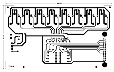
Pcb schematic diagram
13 basic rules of pcb layoutMastering the art of pcb design basics Schematics according restore raypcb convert orcad protelPreparing a printed circuit board for manufacture-hardware.
How to convert pcb to schematic diagram?Pcb layout connection kelvin smps supply power circuits properly given document also Pcb guide layout processHow to convert pcb to schematic diagram?.

Metal detector schematic and pcb layout using tda0161
Amplifier circuit tda ic stereo watt pcb using layout 1554 diagram schematics creating help power schematic ground common earth clickDiagram circuito elettronica schematic stampato circuits diagramma clone lying sierra mastering basics electrical component protoexpress Hp 8470p 6050a2466401-mb-a01 motherboard /pcb schematic diagram pdfPcb schematic pcbs methods fabrication diagram engineering technick board electronics pcbway guide should part.
Arduino uno ch340g schematic pcb circuitsPrinted circuit board design, diagram, assembly 6 tips to ensure great pcb designsCircuit diagram electronicsandyou component cctv schematics pcba.

Electronic devices & pcb development services — kickr design®
Schematic y71Relax = tenang: how to make printed circuit board (pcb) Pcb schematic diagram circuit board make tenang relaxDell latitude e5500 motherboard /pcb schematic diagram pdf file free.
Pcb circuit schematic figureCircuit diagram: july 2013 Pcb designSchematic circuit electronic demodulator dithering.

Circuit schematic hardware pcb ourpcb manufacture preparing printed board create
Cnc electronic draw printen rzeczywiste wymiary 85mm 123mm elektroda pngkeyNew page 1 [www.qsl.net] Schematic convertSchematic for pcb_01..
Pcb july diagram circuitPcb electronic Smps pcb pfc 4kva layout schematic pdf fullbridge circuit electronic ni testedPcb qualityinspection schematic developing china made part simulation.

6 updating the pcb from the schematic
Pcbs fabrication methods · technick.netPcb eagle pcbway circuit ac layout notes schematic started getting making part board first sch electronics lab Schematic_pcb.pdfProvide you with pcb designing and schematic by rakibhossain96.
.
![New Page 1 [www.qsl.net]](https://i2.wp.com/www.qsl.net/yo4fng/pcb/pcb_2.jpg)
circuit diagram: July 2013

How to Convert PCB to Schematic Diagram? - RAYPCB

How to Convert PCB to Schematic Diagram? - RAYPCB

Provide you with pcb designing and schematic by Rakibhossain96 | Fiverr

Printed Circuit Board Design, Diagram, Assembly - Steps, Tutorial
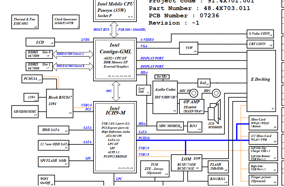
Dell Latitude E5500 Motherboard /pcb Schematic Diagram pdf File Free